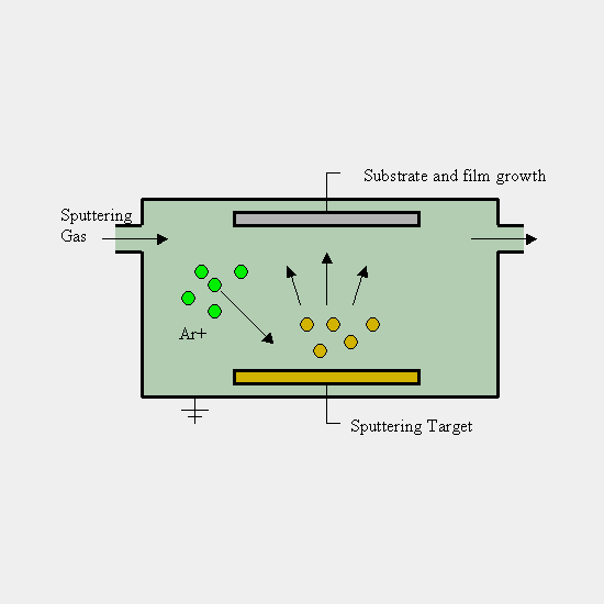
Sputtering is a process used in the field of thin-film deposition, commonly employed in semiconductor manufacturing, optics, and materials science. It involves the removal of atoms or molecules from a solid target material and depositing them onto a substrate to create a thin film. This process is primarily driven by bombarding the target material with high-energy ions, typically from a plasma or gas discharge. As these ions collide with the target, they transfer energy to the target atoms, causing them to be ejected from the surface and deposited onto a substrate, creating a thin film.
Types of Sputtering Techniques:
Sputtering techniques vary based on the method used to dislodge and deposit material onto a target surface. Each type offers unique advantages for specific industrial needs. Below are the common types of sputtering techniques used across different applications:
- DC Sputtering: In this method, a direct current (DC) voltage is applied between the target material and the substrate. The target serves as the cathode, while the substrate is the anode. Argon gas is often used as the sputtering gas.
- RF Sputtering: Radio-frequency (RF) sputtering involves applying an RF power source to create a plasma in the sputtering chamber. This plasma generates high-energy ions, which sputter the target material.
- Magnetron Sputtering: This is a variant of DC or RF sputtering that uses magnets to enhance the process. The magnetic field confines electrons and increases their mobility, leading to higher plasma density and more efficient sputtering.
- Reactive Sputtering: In reactive sputtering, a reactive gas, such as nitrogen or oxygen, is introduced into the sputtering chamber along with the inert gas (usually argon). The target material reacts with the reactive gas, leading to the deposition of compounds on the substrate.
Sputtering targets are the materials that are used as the source for thin-film deposition in the sputtering process. The choice of sputtering target material depends on the desired properties of the thin film and its intended application. Some common sputtering target materials include:
- Metals: Metals like aluminum, copper, gold, silver, and titanium are frequently used for sputtering applications where electrical conductivity or metal coatings are required.
- Semiconductors: Materials like silicon, indium tin oxide (ITO), and gallium arsenide are used for semiconductor device fabrication.
- Dielectrics: Dielectric materials like silicon dioxide (SiO2), silicon nitride (Si3N4), and aluminum oxide (Al2O3) are used for insulating layers and optical coatings.
- Compound Materials: Complex materials, such as oxides, nitrides, and carbides, can be sputtered to create specific properties or compound thin films, e.g., magnetron sputtering of iron oxide for magnetic applications.
- Ceramics: Materials like alumina (Al2O3) and zirconia (ZrO2) can be used for applications requiring hardness, wear resistance, or thermal insulation.
- Superconductors: High-temperature superconducting materials like yttrium barium copper oxide (YBCO) are used for specific research and device applications.
The choice of sputtering target material is essential to control the composition, structure, and properties of the deposited thin film. Researchers and manufacturers carefully select the appropriate target material to meet the requirements of their specific applications.
Read also: What are the Advantages and Applications of Sputtering Techniques?
Conclusion:
In conclusion, sputtering is a vital thin-film deposition method widely used in electronics, optics, and material science. It involves the ejection of atoms from a solid target material, which then deposit onto a substrate to form a thin film. Various sputtering targets—including metals, ceramics, and composite materials—are selected based on the application’s specific requirements, such as conductivity, thermal resistance, and chemical stability. Choosing the right sputtering target is essential to achieving optimal performance and efficiency in coating processes.
We are a USA company catering products and solutions in the USA, Australia, New Zealand, Singapore, Malaysia, India, South Korea, and Vietnam.